Communicate with Supplier? Supplier
cqchuke Mr. cqchuke
What can I do for you?
Contact Supplier
 Email:dorotao@cqzixu.com.cn
Home > Applications > Sapphire, SiC & GaN Applications
Sapphire, SiC & GaN Applications
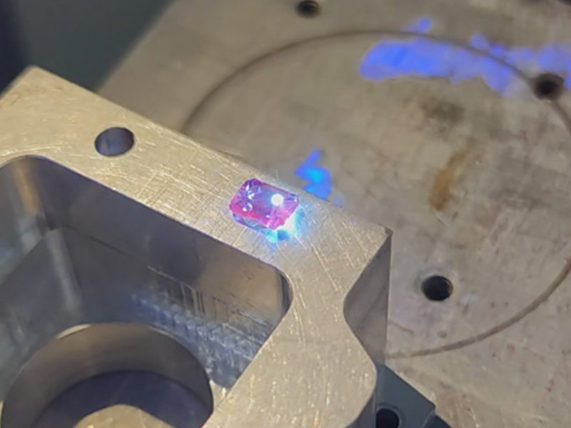
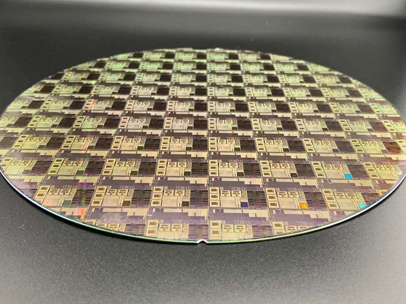
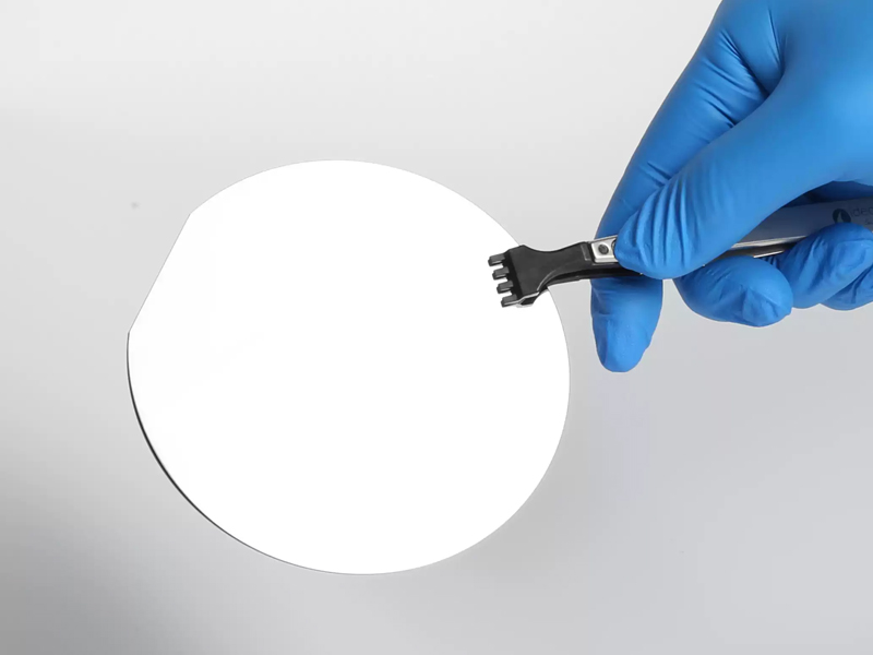
Sapphire (single-crystal Al?O?) and silicon carbide (SiC) are key substrates for high-performance electronic, optoelectronic, and precision optical devices due to their high hardness, thermal conductivity, chemical inertness, and optical transparency. However, traditional processing methods often lead to chipping, microcracks, and tool wear, affecting yield and iteration speed. Therefore, laser processing, with its non-contact and high-precision advantages, has become a core solution, enabling processes such as cutting, dicing, and drilling, transforming these difficult-to-process materials into high-value components.
Precision Micromachining and Material Processing
Ultrafast (picosecond and femtosecond) and high-quality continuous-wave (CW) or quasi-continuous-wave (QCW) fiber lasers have revolutionized the micromachining of sapphire and SiC. The fundamental advantage lies in laser's ability to deliver concentrated energy to a microscale region, either through ultrafast ablation with negligible heat transfer or through controlled thermal processes. This capability is foundational for manufacturing sensor elements, microfluidic channels, and specialized optical components where edge quality and dimensional accuracy are paramount.
Wafer Dicing and Singulation: The Core Industrial Application
Laser dicing methods, such as stealth dicing (SD) and laser ablation dicing, have become industry standards. Stealth dicing employs a focused pulsed laser to form a modified layer of subsurface defects inside the material, followed by a mechanical expansion step to cleave the wafer along this plane. This method produces virtually no chipping, dust, or top-surface damage, maximizes the number of dies per wafer, and is ideal for ultra-thin wafers. Ablation dicing vaporizes material along the cut line with precise control. The transition to laser dicing is a direct response to the need for higher yields, improved device reliability, and the ability to process thinner wafers for advanced packaging.
Overcoming the Hardness Barrier: The Role of Advanced Laser Systems
The successful processing of sapphire and SiC is intensely sensitive to laser parameters. A high-brightness, stable beam allows for consistent focusing to a minute spot size, concentrating energy density to efficiently initiate material removal while minimizing the heat-affected zone (HAZ). This physical principle is the enabler of narrow kerfs and minimal chipping. Furthermore, extensive and precise control over parameters such as pulse frequency, pulse width, and peak power allows process engineers to accurately adjust energy input to accommodate varying substrate thicknesses, crystal orientations, and desired cutting quality.
Surface Engineering and Defect Remediation
Beyond gross material removal, lasers provide a scalpel for modifying surface properties and repairing defects. Controlled laser irradiation can create micro- and nano-scale patterns on sapphire to enhance light extraction in LEDs, increase hydrophobicity, or improve bio-adhesion. Additionally, focused laser beams can be used for localized annealing to heal implantation damage in SiC, activate dopants, or smooth microscopic flaws in sapphire optical windows. 
Broad Application Prospects Across High-End Industries
LED Manufacturing (GaN Epitaxial Substrates):Laser-based low-loss cutting of sapphire protects GaN epitaxy, ensuring brightness and lifespan.High-End Consumer Electronics:Precise shaping and perfect edges combine aesthetics and strength.Semiconductors and 5G Communications:GaN-on-Sapphire RF and SiC power devices feature laser-cut, crack-free edges, maintaining reliability under high electrothermal stress.Advanced Optics and Defense:Military-grade windows and radomes utilize laser depth control processing, preserving material strength and transparency.
In conclusion, the marriage of laser technology with sapphire and silicon carbide substrates represents a cornerstone of advanced manufacturing. It transitions the processing of these "unprocessable" materials from a bottleneck to an enabler. From fundamental micromachining and high-yield dicing to sophisticated surface functionalization, lasers provide the versatile, precise, and controllable toolset required. As industries push toward more miniaturized, efficient, and reliable devices—from brighter LEDs and faster 5G chips to tougher optics and more powerful EVs—advanced laser systems will remain indispensable in unlocking the full potential of these extraordinary materials, driving forward the frontiers of technology.
Please Leave Us A Message
We will contact you

Home

Phone

Skype

Inquiry

绥棱县| 库车县| 大城县| 扶沟县| 阳新县| 嘉祥县| 绥宁县| 永春县| 沈阳市| 什邡市| 忻城县| 七台河市| 宽城| 于都县| 开阳县| 买车| 郴州市| 信丰县| 从化市| 阳泉市| 长阳| 察哈| 当雄县| 东光县| 晋江市| 分宜县| 漠河县| 香港 | 姜堰市| 贵阳市| 保靖县| 江门市| 车险| 福清市| 门源| 昆山市| 永川市| 司法| 安图县| 福州市| 长宁县|